Semiconductor Cleanroom On Semiconductor Cleanroom
For those of you who are automotive hobbyists, you must be familiar with vehicle adjustment
If you are searching about Semiconductor Clean Room Photos and Premium High Res Pictures - Getty you've visit to the right web. We have 17 Images about Semiconductor Clean Room Photos and Premium High Res Pictures - Getty like Cleanroom and Semiconductor – PremiumTech, GlobalFoundries introduces 22nm FD-SOI process technologies | KitGuru and also Patterned 12 Inch 300 Mm Silicon Wafers In A Foup Container Stock Photo. Here it is:
Semiconductor Clean Room Photos And Premium High Res Pictures - Getty
 www.gettyimages.com
clean semiconductor silicon wafer worker electronics portrait royalty
Semiconductor Clean Room Design & Construction Precision Cleanrooms
 precisioncleanrooms.com
semiconductor clean equipment
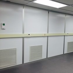
Modular Cleanroom - Portable Clean Rooms For Sale
 www.nationalpartitions.com
cleanroom ducts
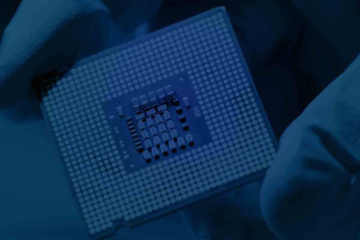
ON Semiconductor Cleanroom | The Pike Company
 www.thepikecompany.com
semiconductor cleanroom
Cleanroom And Semiconductor – PremiumTech
 premiumtech.sg
semiconductor cleanroom
Samsung Semiconductor Profits Rise 80 Percent Thanks To Strong Launches
 www.extremetech.com
samsung semiconductor austin foundry prominent profits percent launches wins rise strong thanks extremetech
Cleanroom For Micro-electronics - HY Cleanroom System Co., Ltd.
 hycleanroom.com
cleanroom electronics micro hy microelectronics ltd project
GlobalFoundries Introduces 22nm FD-SOI Process Technologies | KitGuru
 www.kitguru.net
globalfoundries semiconductor cleanroom soi fd process 22nm 10nm technologies introduces lithography kitguru euv 7nm industry intel beol fab1 space
ASU Nanotechnology Facility For Startups - Cleanroom Connect
 cleanroomconnect.com
nanotechnology asu facility
Chinese Cyber Army Hacked Dutch Chip Maker ASML - Cyberwarzone
 cyberwarzone.com
asml chip cleanroom cyber chinese semiconductor maker hacked army dutch lithography cyberwarzone companies largest
The Value Of Cleanrooms For Semiconductor Applications - Angstrom
 angstromtechnology.com
cleanrooms
Softwall Cleanrooms On Technical Equipment Sales
 products.tesinc.com
softwall cleanroom cleanrooms
Cleanroom For Semiconductor Industry | PortaFab Case Study
 www.portafab.com
semiconductor cleanroom portafab
AMCBP Completes Cleanroom Construction Project For Semiconductor Facility
 amts.com
semiconductor cleanroom construction facility completes project build northeastern hired division performance states 1000 united am
Best Semiconductor Clean Room Stock Photos, Pictures & Royalty-Free
 www.istockphoto.com
semiconductor clean
Semiconductor Clean Room Design & Construction Precision Cleanrooms
 precisioncleanrooms.com
semiconductor cleanrooms clean cleanroom construction
Patterned 12 Inch 300 Mm Silicon Wafers In A Foup Container Stock Photo
 www.istockphoto.com
foup inch silicon mm patterned wafers container istock
Asu nanotechnology facility for startups. Semiconductor clean room design & construction precision cleanrooms. Asml chip cleanroom cyber chinese semiconductor maker hacked army dutch lithography cyberwarzone companies largest
Posting Komentar untuk "Semiconductor Cleanroom On Semiconductor Cleanroom"